
How Does A Convexity Comes Out On Thermoelectric Separation Copper Based PCB?
- Views
- 29 Apr 2024
- What is a Thermoelectric Separation Technology?
- How To Make a Convexity During the PCB Manufacturing?
As technology advances, the requirements for PCBs are also evolved, introducing specialized variants like the thermoelectric separation copper-based PCB. The special for thermoelectric separation PCB is it has convexities on the surface of printed circuit board that can help to transfer heating out through the copper base directly, so that avoiding the overheating of the electronic devices. Today, Best team will introduce the importance of thermoelectric separation copper PCB and how does the convexity come out and its work principle.
What is a Thermoelectric Separation Technology?
A thermoelectric separation copper core PCB, often abbreviated as MCPCB (Metal Core PCB) or SinkPad PCB, is a type of PCB that uses copper alloy as the base core. The term "thermoelectric separation" refers to the PCB’s ability to separate heat generation from the electronic components by conducting it away to avoid performance degradation. The very technology of thermoelectric separation serves in the separation of electrical and thermal paths in such a way that one of them leads to better heat conduction.
Basically, the objective is to reduce thermal resistance in order to achieve efficient heat transfer from the electronic component to the heatsink. This is more critical in the very high heat dissipation devices, e.g., the LED lighting systems, and power converters.
What is the Structure of Thermoelectric Separation Copper PCB?
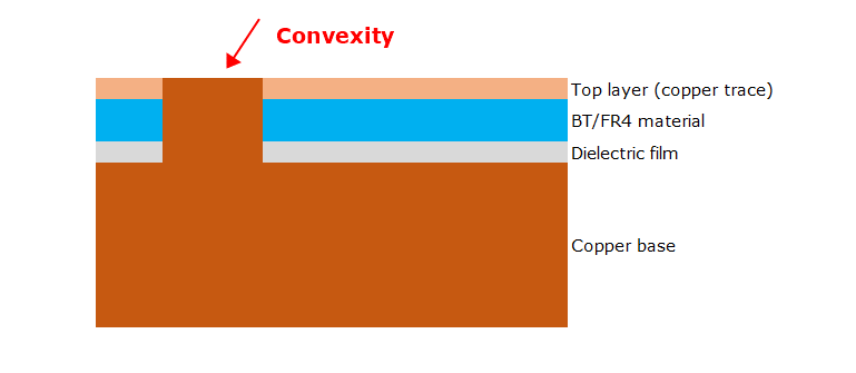
The structure of a thermoelectric separation copper PCB differs significantly from a standard copper PCB, primarily in how it manages heat and electrical conductivity. The key difference lies in its design, where the copper base is structured to form a raised area, or convexity. This convexity is directly connected to the base material, facilitating more efficient thermal management.
This structure allows for improved separation of the thermal and electrical pathways. The raised copper areas serve to concentrate the heat away from critical components, enhancing the overall heat dissipation across the PCB. This design is particularly beneficial in applications where managing high temperatures is crucial, preventing thermal damage and improving the performance and longevity of the electronic components mounted on the PCB. May below stack up of thermoelectric separation copper PCB is easy to make you sense.
How To Make a Convexity During the PCB Manufacturing?
The manufacturing of thermoelectric separation copper PCB is much complex than normal metal core PCB due to the convexity making. First of all, we should know there are two major parts of thermoelectric separation PCB: top trace layer (panel layer) and metal base layer (copper base). Then you will see the manufacturing process of thermoelectric separation copper-based PCB step by step.
1. Manufacturing files preparation
Generally speaking, it is needed to prepare a working gerber (W/G) file first according to the design file for manufacturing when we get it from customers. The main purpose is check whether the trace layer and copper core layer are on a one layer or in different layers. If in the one layer, we should separate them into single different layer, because the convexity and trace layer are made separately.
2. Produce trace layer and metal base layer separately
The trace layer is produced similarly to traditional FR4 PCBs using materials like BT (Bismaleimide-Triazine) or FR4, depending on the application requirements. The copper core layer, however, is prepared differently to accommodate convexities:
l Initial preparation
For normal copper core PCB, the copper base we purchased from supplier is laminated with the dielectric layer, and we make the trace layer on that surface. But for the thermoelectric separation copper PCB, due to the convexity is made on the copper base, laminated copper base is unable to make such convexity but bare copper base is available. The copper base we commonly used thickness is 0.8mm, 1.0mm, 1.2mm, 1.6mm, 2.0mm. To avoid exposure, they always covered with a blue film to protect the surface on both sides, at the first step, we will remove the blue film after raw material cutting and before the convexity making, so that copper can be etched.
l Blue film cover
And then, we will add an extra blue film on the top side of the base and a transparent film on the bottom side to protect the copper (double sided thermoelectric separation copper PCB will cover blue film on the both side). This film is mainly to developing the convexities. After developing and etching, only selected area can be kept, and others can be etched away. Actually, the kept area is the convexity located.
l Copper etching
At this step, the area has blue film is the thermal pad, then we need to etch the copper layer to make it raised. The copper area without protection or transparent film can be etched away and the etch depth will be 0.2-0.25mm. After that, the raised area on the copper base are the convexities.
3. Laminated
Laminated the trace layer and copper core layer together. Before laminated, it is needed to CNC milling a slot for placing convexity on the trace layer, then add a glue (dielectric film) on the bottom of trace layer to stick trace layer with the copper base layer temporarily. After that, the two layers became a whole panel, then we will put it on the lamination machine under high temperature for firmly stick with each other. During this step, the key point is to align the trace layer and metal base layer correctly, make sure the thermal pad is correctly place on its way.
4. Solder mask, silkscreen printing, surface treatment, outline like normal FR4 PCB manufacturing process
Then, the following process is similar to normal FR4 PCB, proceed with solder mask printing, silkscreen printing, surface treatment, outline cutting and FQC process. You can click here to know more about FR4 PCB manufacturing process.
Above are the mainly process of thermoelectric separation copper PCB manufacturing, if you still have some questions about its process, welcome to contact with us, our expert is online 24 hours.
mcpcb, metal core pcb, copper pcb, copper core pcb, sinkpad pcb, thermoelectric separation copper pcb, copper based pcb, thermal management pcb, high power pcb,


Related Blog
- What is Thermal and Electrical Separating Pad in Metal Core PCB?
- LED PCB Assembly Process: Step-by-Step Guide for Beginners
- Why Always Recommend White Solder Mask Black Silkscreen for Aluminum PCB?
- What Materials Are Commonly Used for Manufacturing Lighting PCBs?
- Everything You Should Know About Metal Core Circuit Board
- What Are the Differences Between Ceramic PCB, Metal Core PCB And Standard FR4 PCB?
- Why Choose Best Technology As Your MCPCB Manufacturer?
- What is LED Light Circuit Board and How to Make it?
- When is International Labour Day in 2024 and What are the Significances of It?
- How Does A Convexity Comes Out On Thermoelectric Separation Copper Based PCB?
- Why is Aluminum LED PCB Important for Indoor Growth Lights?
- Application of Metal Core Pcbs in the Development of LED Technology
- Why Choose White Solder Mask for Metal core PCB When Used In LED Devices?
- Understanding Aluminum LED PCBs in 1000w LED Grow Lights
- What Are the Advantages of Metal Core PCB? How to Choose?
- Automotive Light Copper Core Pcb Production Process—testing
- Why Are Metal Core PCBs, Especially Copper Core, Used In Heat-Sensitive Electronics?
- How do aluminum LED PCBs improve LED efficiency?
- What Are the Differences Between Regular and Thermoelectric Separation Copper-Base PCBs?
- Aluminum PCB VS FR-4 Performance Comparison